


PRODUCTS

- PRODUCTS
- MEMS
MEMS
Overview
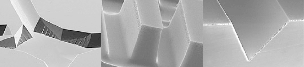
Kodenshi has accumulated experiences for development on optical semiconductor for many years. We have handled Solid processing (MEMS) of silicon, and achieved to release some products into the market.
We can offer various specifications for a solid processing of silicon, basing on the experience for customized specifications to meet the demand of the customers.
The features of MEMS technology by Kodenshi are as follows;
(1)V ditch processing accuracy 1.0μm or less
(2)Possession of “Dry etching technology” and “Wet etching technology”
and the compound technology of “Dry wet etching for silicon crystal unisometric etching technology.
We are well prepared by these technologies corresponding to various demands of the customers!
Solid processing technology of silicon substrate
- ・Consistent development production system from “Micro machining tech.” to “Electrode formation tech.”
- ・Possession of “Dry etching technology” and “Wet etching technology”
- ・The compound technology of “Dry wet etching”.
- ・V ditch processing accuracy 1.0μm or less
MEMS technology of Kodenshi
- Capabilities
-
Silicon crystal unisometric etching technology
Silicon dry etching technology
Silicon wet etching technology
Silicon dry wet etching compound technology
Diamond Fullum formation technology
- Under development
-
The silicon glass joint technology
Technology of process of the glass
Minute electroformed processing technology
Minute reproduction molding technology
- Applications
-
SiOB and optical pass
Micro TAS and micro machining
Micro TAS and micro machining
Micro TAS and micro machining
Flow sensor and pressure sensor
Various sensors
Electrostatic capacity sensor and flow cell
Minute metal mold
Optical pass and lens for optical communication
| Capabilities | Under development | Applications |
|---|---|---|
| Silicon crystal unisometric etching technology | SiOB and optical pass | |
| Silicon dry etching technology | Micro TAS and micro machining | |
| Silicon wet etching technology | Micro TAS and micro machining | |
| Silicon dry wet etching compound technology | Micro TAS and micro machining | |
| Diamond Fullum formation technology | Flow sensor and pressure sensor | |
| The silicon glass joint technology | Various sensors | |
| Technology of process of the glass | Electrostatic capacity sensor and flow cell | |
| Minute electroformed processing technology | Minute metal mold | |
| Minute reproduction molding technology | Optical pass and lens for optical communication |
Execution example
The MEMS technology of Kodenshi is made the best use of in customer’s specification. Please do not hesitate to inquire details.
You will find a KODENSHI MEMS technology that is really close to what you are looking for.To find out more about KODENSHI custom product development capabilities,please contact us.KODENSHI is always at your service.